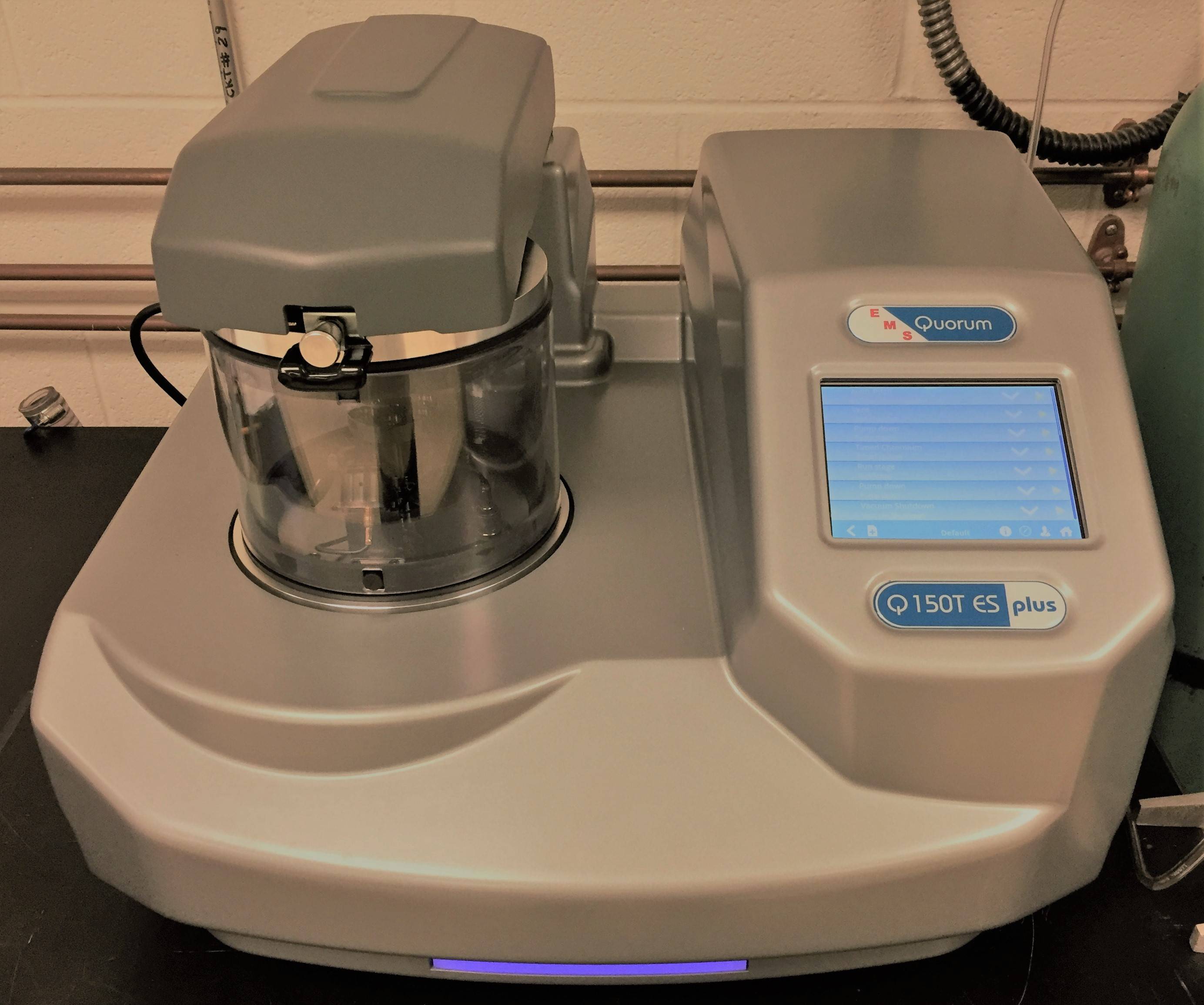
EMS 550X Sputter Coater
What is Sputter Coating?
To visualize samples by scanning electron microscopy, samples need to be conductive to prevent the accumulation of electric charges on their surface when hit by the electron beam used for imaging. Some samples (e.g. some metals) are naturally conductive while other (e.g. ceramics, biological samples) are not. Charges will accumulate on non-conductive samples and this will alter the trajectory of the electrons in the beam and result in image distortions.
Sputter coating is the process by which samples are coated with a thin layer of conductive material. Sputter coating is a physical vapor thin film deposition method in which atoms are vaporized from a solid target and deposited on a sample to form a solid, conductive layer. In addition to reducing sample charging, sputter coating also improves secondary electrons emission, protects electron sensitive samples, reduces beam penetration and improves edge resolution.
The parameters to consider when performing sputter coating include the material for deposition and the thickness and grain size of the deposited layer. Gold/Palladium (80:20) is the most common choice for routine coating of a wide range of samples. Palladium acts as a physical barrier to prevent the gold to form large clusters at the surface of the sample. Typically, the thickness of the coating is 2 nm. Material other than gold/palladium, such as carbon, chromium, silver, etc. may be used for sputter coating depending on whether the sample is to be analyzed by EDAX or BSE imaging.
Features & Specifications of the EMS 550X Sputter Coater
- Fully automatic control
- Low voltage sputtering
- High resolution fine coating (order of 2nm gold grain)
- Special rotating stage with full tilt facility fitted as standard
- Even thickness deposition (typically 20nm or 200 Angstroms for SEM work)
- 165 mm diameter (6 inches) chamber
- Borosilicate work chamber dimensions: 165 mm dia x 125 mm high
- Polycarbonate safety shield
- Target dimensions: 60 mm dia x 0.1 mm thick
- Specimen stage: 60mm Dia., Rotating with tilt facility, spacing to target 40 mm
- Vacuum Gauge Range ATM - 1x10⁻⁴ mbar
- Deposition range 0-50mA
- Deposition rate 0-25nm/minute
- Sputter timer 0-4 minutes

