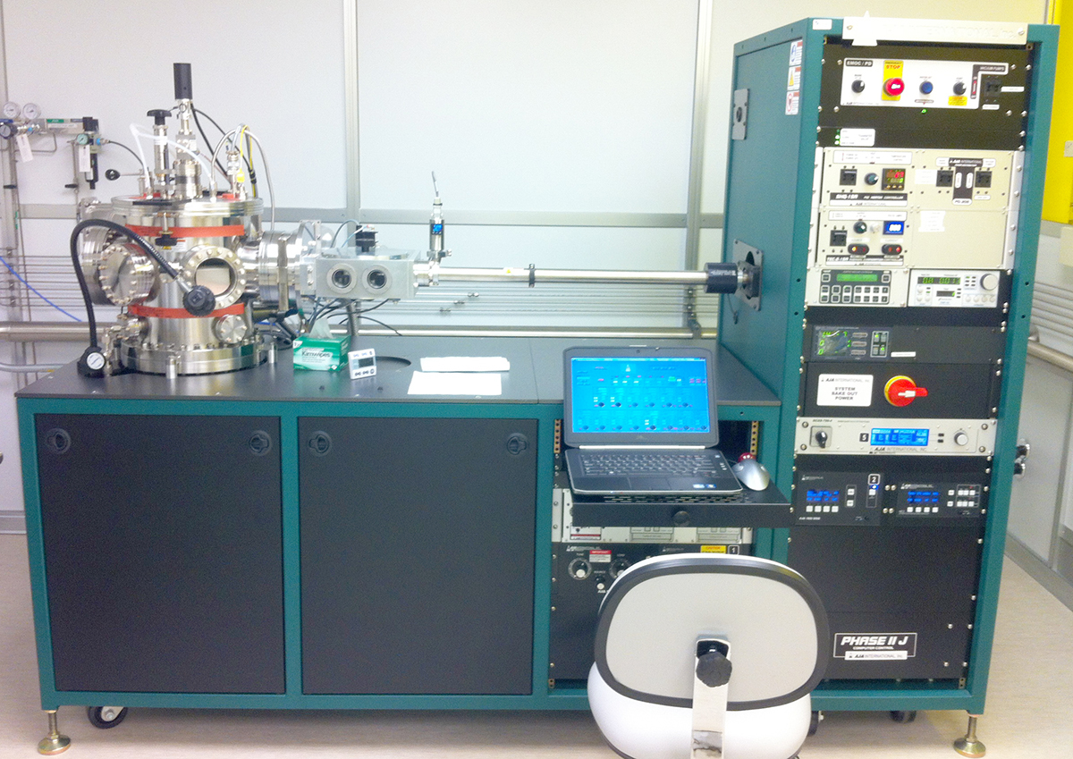
What is a Deposition Unit?

The deposition unit deposits thin films on a surface by sputtering. Sputtering involves eroding material from a target or source onto a substrate, such as a silicon wafer or glass. Sputtering has many applications. In the semiconductor industry, it is used to deposit thin films of various materials during the manufacturing of integrated circuits or to deposit contact metals for thin film transistors. Deposition units also serve to create thin antireflection coatings on glass for optical applications.
Major Features and Specifications of the AJA Orion 5
- Can be used as a sputtering system as well as a thermal evaporator using a single sample holder.
- Deposits metal and dielectric films from three source targets to substrates using ionized gas (Ar and N2)
- Fitted with 3 guns powered by RF and DC sources
- Can be used for single- or multi-layer deposition.
- (Other 4 bullet points that are already on the web)
- Designed to accommodate wafers up to 4² (~100 mm) in diameter
- One dc and two rf power sources for the sputtering targets
- Three 2.5² (~63.5 mm) diameter sputter guns
- Substrate heating to 850°C
- Substrate rotation
- Substrate biasing for cleaning
- Main-chamber base pressure 8x10⁻⁸ Torr or better
Users interested in using the Materials Science Lab or equipment should contact:
